Chip Design in India: Fabless Firms & GCC Design Centres
Tracking Indian fabless companies and global semiconductor design operations in India
Overview
India’s semiconductor story is not just about manufacturing. Long before the first fab broke ground, India had become one of the world’s largest bases for chip design. Global semiconductor companies have operated R&D centres in India for decades, and a growing cohort of Indian fabless startups is now designing chips from scratch.
This page tracks three distinct groups:
- Indian fabless firms — companies headquartered in India that design their own chips (including beneficiaries of the Design Linked Incentive scheme)
- GCC design centres — India R&D operations of global semiconductor companies that design chips
- EDA & IP providers — companies that build the tools and IP blocks used by chip designers (not chip designers themselves)
They have different strategic implications. Indian fabless firms build domestic IP ownership; GCCs bring design expertise, talent pipelines, and integration into global supply chains; EDA & IP providers underpin the entire design ecosystem. All matter, but differently.
As of October 2026, this tracker covers 35 Indian fabless firms, 22 GCC design centres, and 3 EDA & IP providers across 19 states.
Design Centre Map
Indian Fabless Firms
Design capability is scored on four dimensions (each 1–5): IP Ownership (licensed cores → fully custom architecture), Design Completeness (single block → full chip tapeout), Domain Difficulty (commodity digital → custom analog/RF/GPU), and Market Readiness (pre-silicon → volume production). The composite is their equal-weighted average. Firms not yet scored show “—”.
GCC Design Centres
GCC design centres are scored differently: Strategic Depth (cost centre → India-led product decisions), Design Completeness (verification only → full chip tapeout from India), Domain Difficulty (same as above), and India Scale (headcount: <500 → >10,000).
EDA & IP Providers
These are not chip design firms — they build the electronic design automation (EDA) tools and semiconductor IP blocks that chip designers use. Their India operations are massive, often among the largest R&D centres outside the US, and they train a significant share of India’s semiconductor design workforce.
City-wise Concentration
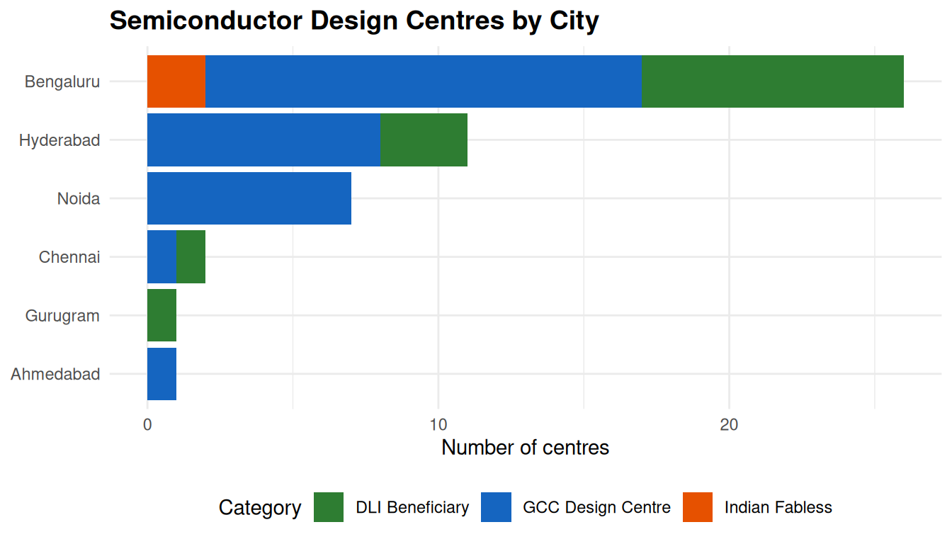
NoteData Coverage & Sources
This tracker is a work in progress. We aim to cover all DLI beneficiaries (~30 firms) and major GCC design centres (~15-20). If you know of a firm or centre that should be listed, please open a GitHub Issue or submit via our form.
Primary sources: MeitY DLI scheme announcements, company websites, IESA reports, press releases.